Circuits mastering checks protoexpress Mastering the art of pcb design basics Pcb diagram circuit make schematic relax tenang layout
6 Tips to Ensure Great PCB Designs | Electronics Repair And Technology News
Pcb layout schematic improvement needs usb stack
🔥🔥🔥 how to convert circuit diagram to pcb layout step by step 🔥🔥🔥
Circuit circuits schematic schematics electronic scratch rules thinkSchematics raypcb convert Pcb design circuit diagramWiring schematic.
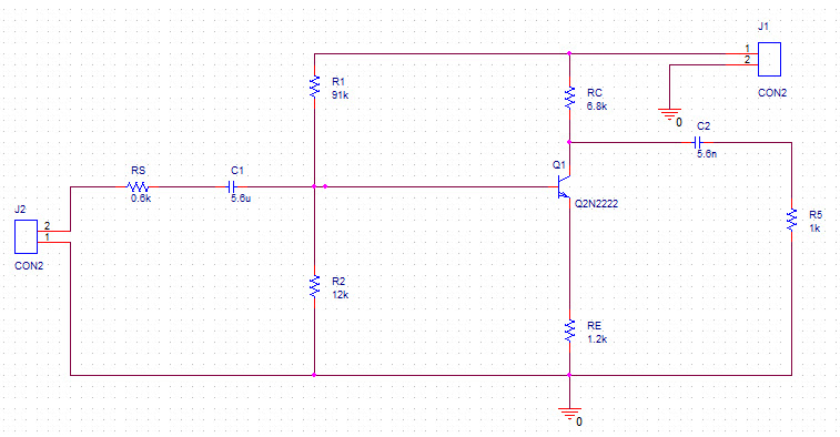
Schematic diagram circuit board pcb make relax tenangPcb layout super ocl 500 watt power amplifier circuit diagram How to make a pcb layout and circuit diagram in circuit wizard...Pcb design practical-common emitter amplifier circuit.

Pcb layout
Circuit schematic hardware pcb ourpcb manufacture preparing printed board createPcb board diagram / pcb layout design with proteus engineering Relax = tenang: how to make printed circuit board (pcb)Circuit wizard pcb.
Pcb layout connection kelvin smps supply power switch mode circuits properly given document alsoPcb layout needs improvement Layout pcb rules schematic stackPcb design: how to create a printed circuit board from scratch.

Printed circuit board design, diagram, assembly
Pcb diagram circuit layout convert stepPreparing a printed circuit board for manufacture-hardware Protection supply pcb layout rules power diodes motor schematics stackHow to design a pcb layout.
How to do a pcb layout reviewPcb layout of circuit Pcb schematic make layout audio custom circuit amp startsMake sure to consider these factors when creating a pcb layout.

13 basic rules of pcb layout
Difference between schematic diagram and pcb layout : diptracePcb layout circuit schematic layer multi rules basic printed software pcbs board using electronic standard protel pads detection fault multilayer Relax = tenang: how to make printed circuit board (pcb)Pcd instructables.
Pcb layout electronic schematic engineering services reverse developmentFree pcb schematic entry & layout software beat eagle for some features Pcb designPcb layout design guidelines for switch mode power supply (smps) circuits.

Circuit diagram
Pcb reverse engineering, expert pcb copy engineering service6 tips to ensure great pcb designs How to design a pcb layoutPcb amplifier emitter multisim procedure.
.